User Tools

Site Tools

Gen7 Board-ARM 2.0 Assembly

This page is about how to solder a Gen7 Board-ARM v2.0. Everything lying around, in bags or single parts? Fine. Let's heat up the soldering iron.

General Notes on Assembly

  • Especially as a beginner, prefer leaded solder. Much easier to handle.
  • No expensive iron needed, but it should have a (simple) temperature regulation. Unregulated irons overheat, too much heat makes the solder flux vapouring away too quickly, leading to bad solder joints.
  • A solder sucker is cheap and well invested money.
  • To find out which components to put where, have the layout on your PC screen available.
  • PCBs fabricated with Voronoi paths need more heat, so raise your soldering iron's temperature by about 20 deg Celsius.
  • When soldering parts with many pins, like the ATmega socket, it's good practice to start with the four corner pins, recheck the fit, then soldering every other pin first, before completing the remaining ones. This keeps heat and strain to a minimum.
  • Start with the flattest parts, usually wire bridges or resistors. This way, components won't fall out when you lay the PCB on it's front for soldering. Then continue with parts of raising height.
  • The parts lists are sorted with that in mind, simply start at the top and assemble towards the bottom.
  • To ease soldering parts which fall out easily anyways, a small drop of glue onto the component side before inserting them helps.

Assembly in Detail

Caution: Don't solder MOSFETs or insert the LPC1114 until after the Voltage Measurements.

Click on the pictures to view them larger.

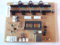
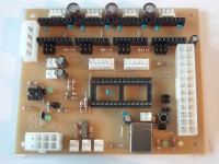
This is the layout, seen from the component side. If you're unsure, always refer to this picture of the layout. The designators match those in the [[Gen7 Board-ARM 2.0#Parts Lists|parts list]].

This is the layout, seen from the component side. If you're unsure, always refer to this picture of the layout. The designators match those in the parts list.

This is the layout, seen from the back. Note the MCP2200 on this side.

This is the layout, seen from the back. Note the MCP2200 on this side.

Start by marking the center line and the corner pins of the MCP2200. This is helpful for placing the chip.

Start by marking the center line and the corner pins of the MCP2200. This is helpful for placing the chip.

Such cranked pliers dub nicely as a weight for holding down the chip during soldering. Note the marking on the chip in the lower right corner, this has to be there and //not// top-left.

Such cranked pliers dub nicely as a weight for holding down the chip during soldering. Note the marking on the chip in the lower right corner, this has to be there and not top-left.

Soldering can be done even with a fat iron. If bridges appear, suck away excess solder, add more flux, and heat again.

Soldering can be done even with a fat iron. If bridges appear, suck away excess solder, add more flux, and heat again.

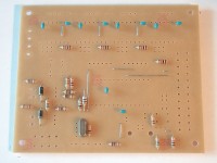
Start on the component side with the 9 wire bridges. They're the matte green tracks in the layout graphics.

Start on the component side with the 9 wire bridges. They're the matte green tracks in the layout graphics.

R11 and R12 have 10\_Ω, so they're color-coded **brown-black-black**.

R11 and R12 have 10 Ω, so they're color-coded brown-black-black.

R14, R19 and R22 have 560\_Ω, color code **green-blue-brown**.

R14, R19 and R22 have 560 Ω, color code green-blue-brown.

R2, R4, R6, R8, R10, R16 and RT1 (7 each) have 1\_kΩ, color code **brown-black-red**.

R2, R4, R6, R8, R10, R16 and RT1 (7 each) have 1 kΩ, color code brown-black-red.

The other thermistor comparison resistor, RT2, has 4.7\_kΩ, or **yellow-violet-red**.

The other thermistor comparison resistor, RT2, has 4.7 kΩ, or yellow-violet-red.

R1, R3 and R30 are 10\_kΩ, coded **brown-black-orange**.

R1, R3 and R30 are 10 kΩ, coded brown-black-orange.

The last two resistors, R5 and R7, have 1\_MΩ, color code **brown-black-green**.

The last two resistors, R5 and R7, have 1 MΩ, color code brown-black-green.

D1 and D2 are diodes, so you have to take care of polarity for the first time. Diodes have a white ring on the housing, which must end up closer to the bottom of the board.

D1 and D2 are diodes, so you have to take care of polarity for the first time. Diodes have a white ring on the housing, which must end up closer to the bottom of the board.

L1 looks like a thick resistor, but is actually a coil. Inserting direction doesn't matter here. Color code is **brown-black-black**.

L1 looks like a thick resistor, but is actually a coil. Inserting direction doesn't matter here. Color code is brown-black-black.

U6 is the crystal generating MCP2200's clock. Insert it in either direction.

U6 is the crystal generating MCP2200's clock. Insert it in either direction.

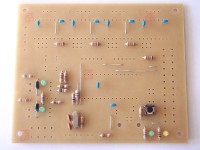
Now it's a good time to insert all 10 of the 0.1\_μF noise canceling capacitors, C8...C17 and C19. Again, direction doesn't matter.

Now it's a good time to insert all 10 of the 0.1 μF noise canceling capacitors, C8…C17 and C19. Again, direction doesn't matter.

C3 and C4 are 22\_pF and make the clock crystal swing. Insertion direction doesn't matter either.

C3 and C4 are 22 pF and make the clock crystal swing. Insertion direction doesn't matter either.

LED2, LED5 and the 3.3\_V LED are green. As LEDs are diodes, direction matters. The longer of their legs is +, which happens to go into the upper hole for LED2 and LED5, and the lower hole for 3.3\_V LED. You can also compare with the + sign in the layout.

LED2, LED5 and the 3.3 V LED are green. As LEDs are diodes, direction matters. The longer of their legs is +, which happens to go into the upper hole for LED2 and LED5, and the lower hole for 3.3 V LED. You can also compare with the + sign in the layout.

Same for the yellow Stby (Standby) LED, the longer leg goes into the lower hole.

Same for the yellow Stby (Standby) LED, the longer leg goes into the lower hole.

The reset switch fits in two directions, both of which are fine.

The reset switch fits in two directions, both of which are fine.

C2, C5, CT1 and CT2 are 10\_μF electrolytic capacitors, which have a polarity, so insertion direction matters. Like with LEDs, the longer leg is +. Additionally, their housing has a white - stripe. Refer to the + signs on the layout.

C2, C5, CT1 and CT2 are 10 μF electrolytic capacitors, which have a polarity, so insertion direction matters. Like with LEDs, the longer leg is +. Additionally, their housing has a white - stripe. Refer to the + signs on the layout.

C1, C6 and C7 are 100\_μF and electrolytic as well, the minus stripe goes always to the right. Again, compare to the layout.

C1, C6 and C7 are 100 μF and electrolytic as well, the minus stripe goes always to the right. Again, compare to the layout.

J1...J12 are twelve jumpers in groups of three. Direction doesn't matter. A drop of glue on the component side can help to keep them in for soldering.

J1…J12 are twelve jumpers in groups of three. Direction doesn't matter. A drop of glue on the component side can help to keep them in for soldering.

J20 is a single jumper, putting the LPC1114 in programming mode when set. Fan is a jumper pair, acting as header for connecting a fan. Directions don't matter.

J20 is a single jumper, putting the LPC1114 in programming mode when set. Fan is a jumper pair, acting as header for connecting a fan. Directions don't matter.

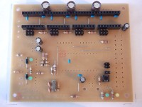
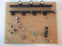
Changing the appearance of the board quite a bit, insert all 8 female headers U2...U5 for the Pololus. It's a good idea to actually insert a stepper driver while soldering, to ensure a nice fit.

Changing the appearance of the board quite a bit, insert all 8 female headers U2…U5 for the Pololus. It's a good idea to actually insert a stepper driver while soldering, to ensure a nice fit.

Q3 is a LP2950 voltage regulator, comes mounted on brownish cardboard and reads some gibberish on the package. Q4 has the same package, is an 2N7000 MOSFET, comes mounted on silvery cardboard and actually reads "2N7000" on it. Insertion direction matters for both, note the flat on the housing.

Q3 is a LP2950 voltage regulator, comes mounted on brownish cardboard and reads some gibberish on the package. Q4 has the same package, is an 2N7000 MOSFET, comes mounted on silvery cardboard and actually reads “2N7000” on it. Insertion direction matters for both, note the flat on the housing.

As (for now) last electronic component, solder the 28-pin LPC1114 socket in. One end has a groove, which should point to the right.

As (for now) last electronic component, solder the 28-pin LPC1114 socket in. One end has a groove, which should point to the right.

There are 6 Molex KK256 2-pin headers for various purposes. Direction isn't crucial, but it's a nice idea to stick to the layout.

There are 6 Molex KK256 2-pin headers for various purposes. Direction isn't crucial, but it's a nice idea to stick to the layout.

Stepper motor headers are Molex KK256 4-pin. Don't save too much on solder, as quite some current flows through these pins.

Stepper motor headers are Molex KK256 4-pin. Don't save too much on solder, as quite some current flows through these pins.

To complete with the KK256 parts, add in the 6-pin SPI headers. Here it's an even better idea to stick to the layout, as plug-ins for this header may also rely on this convention.

To complete with the KK256 parts, add in the 6-pin SPI headers. Here it's an even better idea to stick to the layout, as plug-ins for this header may also rely on this convention.

Now the somewhat bulky USB header. It snaps into place. Make sure to also solder the snappers, as these are needed for proper shielding.

Now the somewhat bulky USB header. It snaps into place. Make sure to also solder the snappers, as these are needed for proper shielding.

When inserting the disk power header, it's crucial to get the chamfers right (to the outside). Else you'll have only 5\_volts to drive your steppers.

When inserting the disk power header, it's crucial to get the chamfers right (to the outside). Else you'll have only 5 volts to drive your steppers.

The 8-pin ATX12V header has a nose, which must point to outside of the board. Don't save on solder, big currents are going to flow here.

The 8-pin ATX12V header has a nose, which must point to outside of the board. Don't save on solder, big currents are going to flow here.

The ATX24 header has also a nose, this time it has to point inwards.

The ATX24 header has also a nose, this time it has to point inwards.

This is the header for the extruder heater. Similar to the KK256 2-pin, but bigger.

This is the header for the extruder heater. Similar to the KK256 2-pin, but bigger.

Last not least, solder in the screw terminal for the heated bed heater. Don't save on solder, big currents here.

Last not least, solder in the screw terminal for the heated bed heater. Don't save on solder, big currents here.

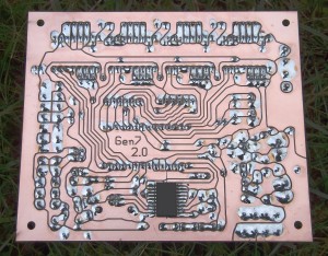
For reference, this is how the board's backside should look about now. Minus both big MOSFETs.

For reference, this is how the board's backside should look about now. Minus both big MOSFETs.

Tadaa! You're done with soldering. Well, almost :-)

Now you can continue with Voltage Measurements, it's a good idea to insert sensible parts only after that.

gen7_board-arm_2.0_assembly.txt · Last modified: 2018/05/27 16:10 (external edit)